Cheon, Master\'s Degree Course Student at the School of Materials Science and Engineering, Develops New Material that can Improve the Semiconductor Process N
No.88404- Writer YU
- Date : 2011.05.11 10:03
- Views : 11320
New material to overcome limitations of nano sized semiconductor copper wires process
US Physics Society selects as paper with academic value in the world\'s published theses in the nano sector
Domestic Patent registered, and preparing to register for international patent
[March 24, 2011]
“With the size of semiconductors becoming nano sized (10⁻⁹), it has become difficult to fill copper, which is a conductive material, in the wiring for the current semiconductor manufacturing process, and has also resulted in the limitations caused by increased resistance. After one year of research to overcome this, it was possible to develop an epochal new material that can simplify the process, while enhancing performance. The fundamental solution to this was accurately understanding the property and properly utilizing it.\"
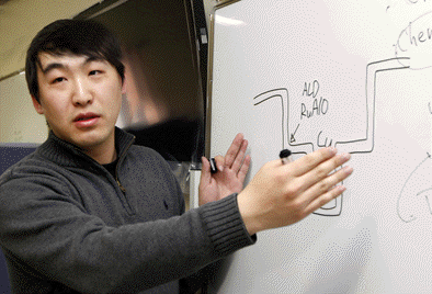
Cheon, Tae-hoon (29, Master\'s degree course, photo), who is currently in the YU Graduate School of Materials Science and Engineering, recently developed a new material that can greatly reduce the stages for semiconductor processes. He became the first to develop the new material \'RuAlO\', which can replace the three layers (diffusion prevention layer, seed layer) that covers the copper wiring in semiconductors, with just one layer.
\'RuAlO\' is a metallic material that was combined through the ALD (atomic layer deposition) of ruthenium (Ru) and ALD of aluminum oxide. When using this in the semiconductor process, it can not only sufficiently obtain space to install copper wires in semiconductor materials that are lower than 20nm, but also make direct plating of a thin layer on the copper wiring using the principle of electrolysis on top of this material, which can thus improve the properties of copper wires. It can also reduce resistance to minimize the size of the semiconductor materials, while also improving performance.
Such achievement was made during the process of the ultra-fine/highly-reliable wiring technology development project, which was part of the \'industrial platform technology development project\', in which the Ministry of Knowledge Economy invests 2 billion won annually since March of last year. This was published in the international society last year, and caused quite a stir. Its value was recognized in early March by being published in the SCI-level international journal ≪Electrochemical and Solid-state Letters≫ (March 8).
Also, on the 21st of this month, it was also published in the ≪Virtual Journal Of Nanoscale Science & Technology≫ co-published by the American Physical Society and American Institute of Physics. The ≪Virtual Journal Of Nanoscale Science & Technology≫ selects about 90 papers with great academic value among papers published around the world on the subject of nano and publishes them weekly. Cheon\'s paper received great interest from the international academic circles, as well as the semiconductor industry, after being published a week before. It is also being scheduled to be presented at the \'Materials Research Society\', which is the world\'s largest international academic conference on the materials sector, in San Francisco next month.
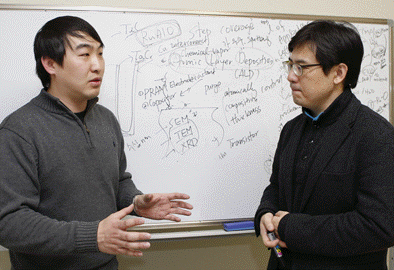
Professor Kim, Soo-hyun (37, School of Materials Science and Engineering, right on photo), who was the advisor for the paper, stated, \"It is a great feat for a student in his master\'s degree program to have his paper selected with other papers in ≪Nature≫ or ≪Science≫ in the nano sector.\" Kim added, \"It is a great achievement in the semiconductor wiring process, which had become limited in procuring better performance during the course of reducing the size of semiconductors in order to enhance performance and degree of integration.\"
Cheon, who is currently working as a TA at the YU Center for Research Facilities, is highly interested in understanding the properties of materials by utilizing various analysis techniques. He stated that he would like to continue research even after completing his studies, and said, \"We have already completed registration for domestic patents for the RuAIO that we developed, and we are currently getting ready to apply for an international patent. I am planning to continue experimenting to see if it can be used in other fields as well.\" He also added with a big smile, \"All new technologies are born through thorough understanding of the properties of the material, and various attempts at its application, and numerous trials and errors. Research on material properties, which is the basis for precision analysis, is very important and worth.\"
※ Atomic layer deposition: IT Dictionary
Nano film attachment technology using the monoatomic layer that is chemically attached during the semiconductor manufacturing process. By repeatedly performing the adhesion and transposition of molecules on a wafer, it becomes possible for atomic layer-width ultra-fine layer-by-layer deposition, and oxide and metal film can be piled up at minimal thickness. In addition, because the particles made through the chemical reaction of gases can create a layer at a temperature lower than Chemical Vapor Deposition (CVD) at below 500 degrees, in which it is deposited on the wafer surface, it is suitable for SoC (system on chip) production. As a leader in high-technologies, Korea is at a leading position and exports core technologies.